[[PERFORMANCE_et+al_NvidiaH100TensorCoreGpu_2022]]
#finding/#nvidia; #nvidia; #streaming_multiprocessor; #artificial_intelligence; #TFLOPS; #high_performance_computing; #speed_up; #general_purpose; #thermal_design_power; #_general; #gpu_computing
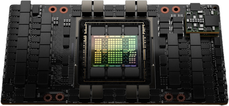
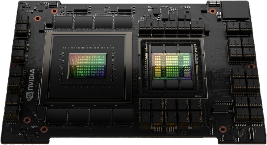
In this whitepaper we introduce the new NVIDIA H100 Tensor Core GPU, our next-generation, highest-performing data center GPU
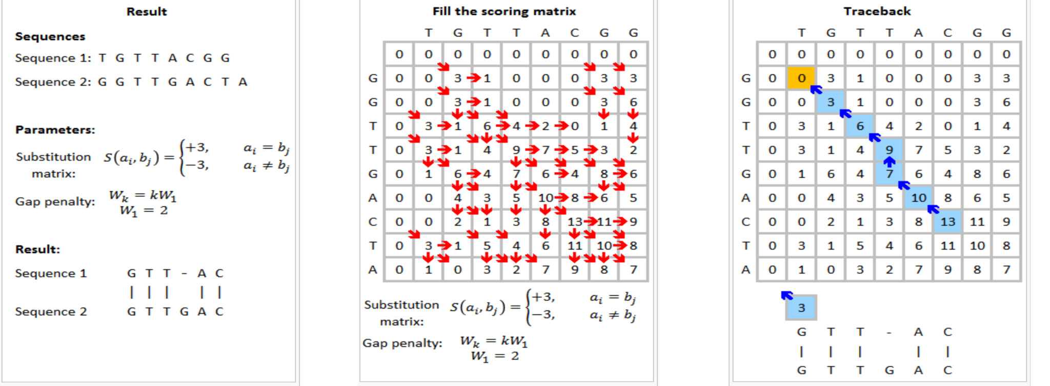
![Figure 36. Smith-Waterman Algorithm for Genome sequencing[^1]](https://scholarcy.nyc3.digitaloceanspaces.com/images/104778/nvidia-h100-tensor-core-hopper-whitepaper/img-063.png)
- Introduction to the NVIDIA
H100 Tensor Core GPU - Accelerated computing requires more than just powerful GPUs
- CUDA tools and libraries have been downloaded over 30 million times and used by nearly 3 million developers
- The CUDA platform has been continuously improved, optimized, and expanded with more powerful CUDA-enabled GPUs, new and diverse sets of GPU-accelerated libraries, workstations, servers, and applications to broaden the reach of NVIDIA accelerated computing
- One of the largest supercomputing endeavors will be NVIDIA’s own Earth-2 Supercomputer project which will continuously stream enormous amounts of data into a digital twin of the Earth running physical simulations in Omniverse to predict future weather patterns worldwide. In this whitepaper we introduce the new NVIDIA H100 Tensor Core GPU, our next-generation, highest-performing data center GPU
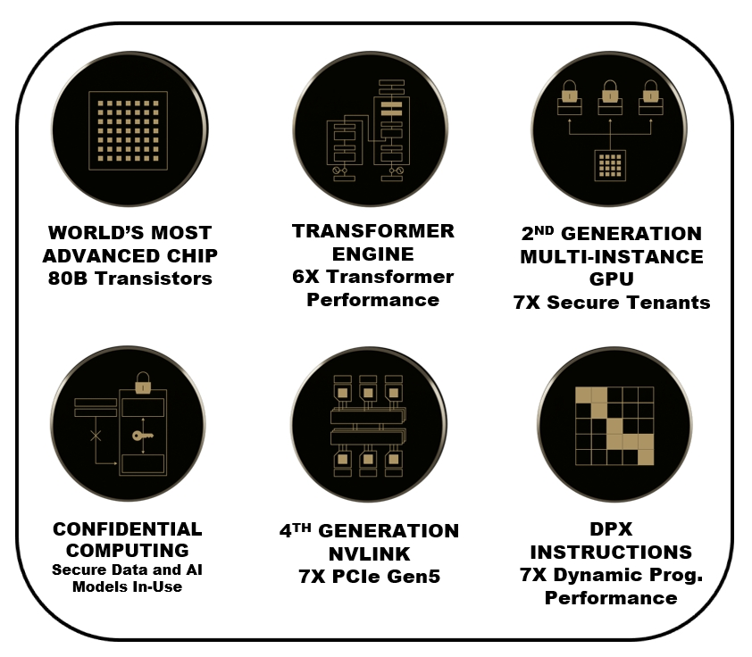
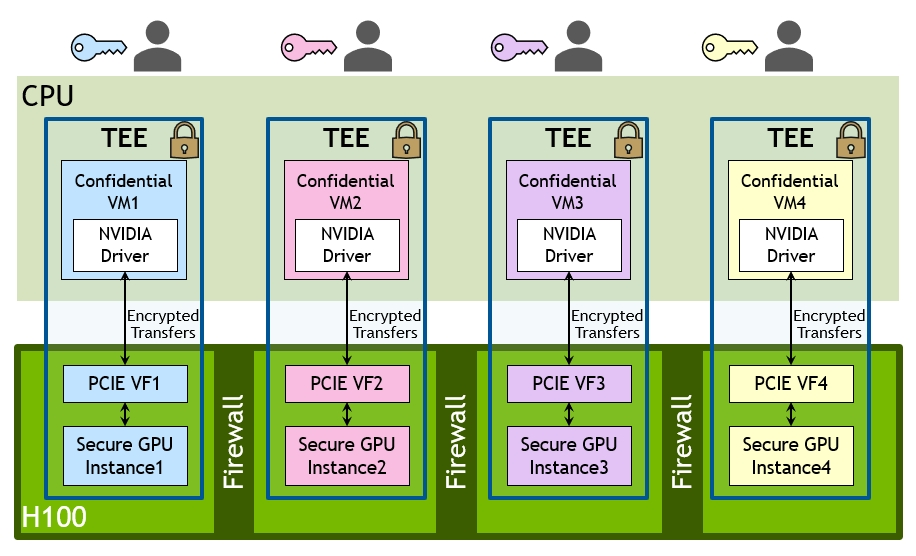
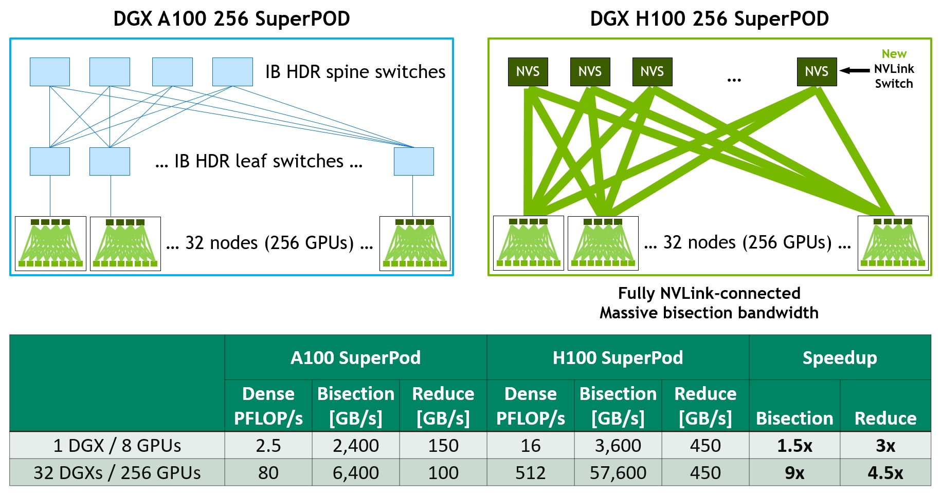
- H100 implements the world's first native Confidential Computing GPU and extends the Trusted Execution Environment with CPUs at full PCIe line rate. ● Fourth-generation NVIDIA NVLink® provides a 3x bandwidth increase on all-reduce operations and a 50% general bandwidth increase over the prior generation NVLink with 900 GB/sec total bandwidth for multi-GPU IO operating at 7x the bandwidth of PCIe Gen 5. ● Third-generation NVSwitch technology includes switches residing both inside and outside of nodes to connect multiple GPUs in servers, clusters, and data center environments
- New third-generation NVSwitch technology provides hardware acceleration for collective operations with multicast and NVIDIA SHARP in-network reductions. ● New NVLink Switch System interconnect technology and new second-level NVLink Switches based on third-gen NVSwitch technology introduce address space isolation and protection, enabling up to 32 nodes or 256 GPUs to be connected over NVLink in a 2:1 tapered, fat tree topology
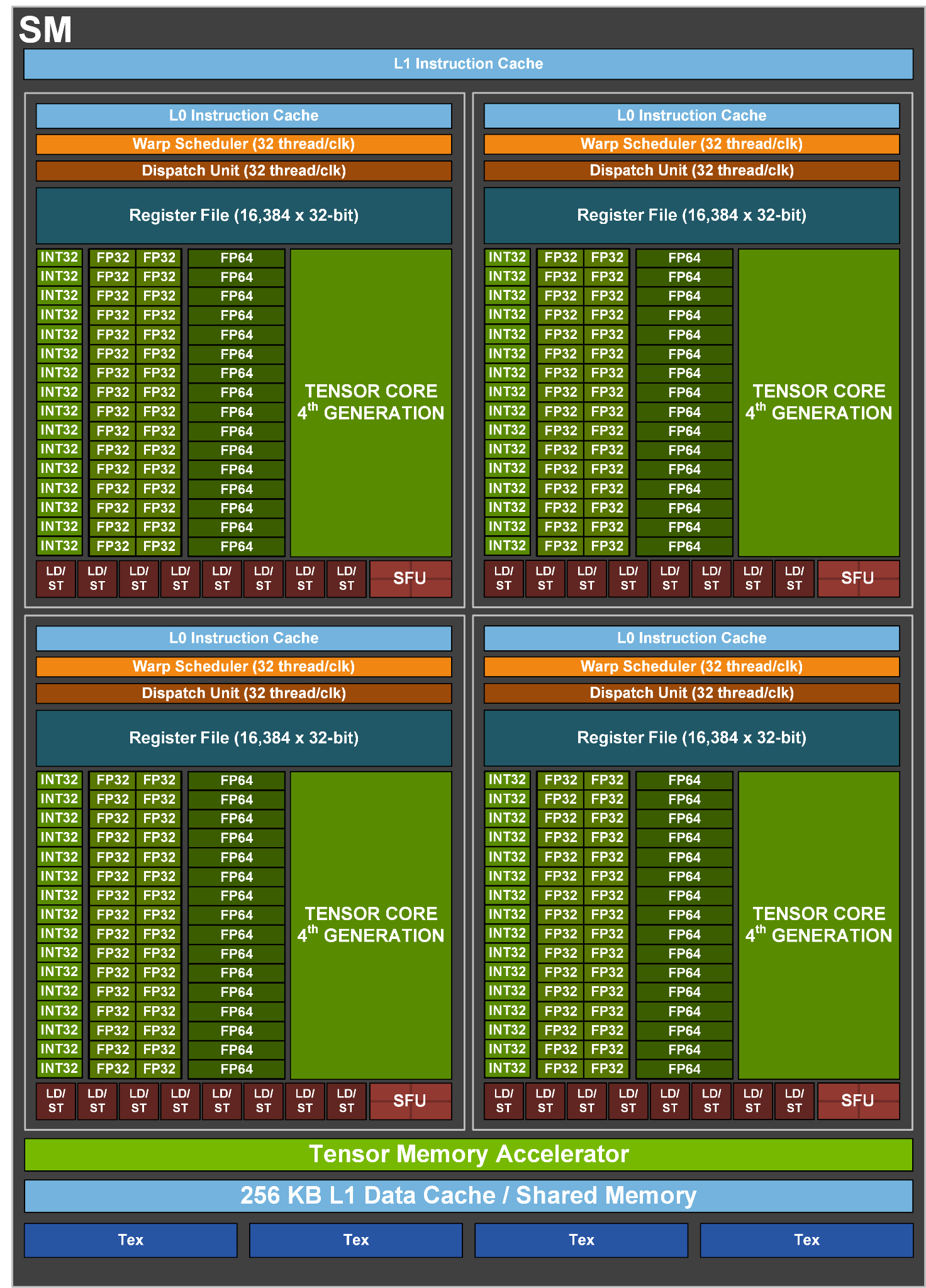
- Tensor Cores operating in parallel across Streaming Multiprocessor (SM) in one NVIDIA GPU deliver massive increases in throughput and efficiency compared to standard Floating-Point (FP), Integer (INT), and FMA (Fused Multiply-Accumulate) operations
Accelerated computing requires more than just powerful NVIDIA CUDA tools and libraries have been downloaded over 30 million times and used by nearly 3 million developers. One of the largest supercomputing endeavors will be NVIDIA’s own Earth-2 Supercomputer project which will continuously stream enormous amounts of data into a digital twin of the Earth running physical simulations in Omniverse to predict future weather patterns worldwide. In this whitepaper we introduce the new nVIDIA H100 Tensor Core GPU, our next-generation, highest-performing data center NVIDIA H100 implements the world’s first native Confidential Computing GPU and extends the Trusted Execution Environment with CPUs at full PCIe line rate. H100 implements the world's first native Confidential Computing GPU and extends the Trusted Execution Environment with CPUs at full PCIe line rate. Fourth-generation NVIDIA NVLink provides a 3x bandwidth increase on all-reduce operations and a 50% general bandwidth increase over the prior generation NVLink. Third-generation NVSwitch technology includes switches residing both inside and outside of nodes to connect multiple GPUs.
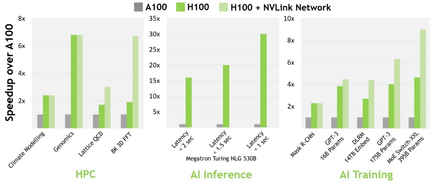
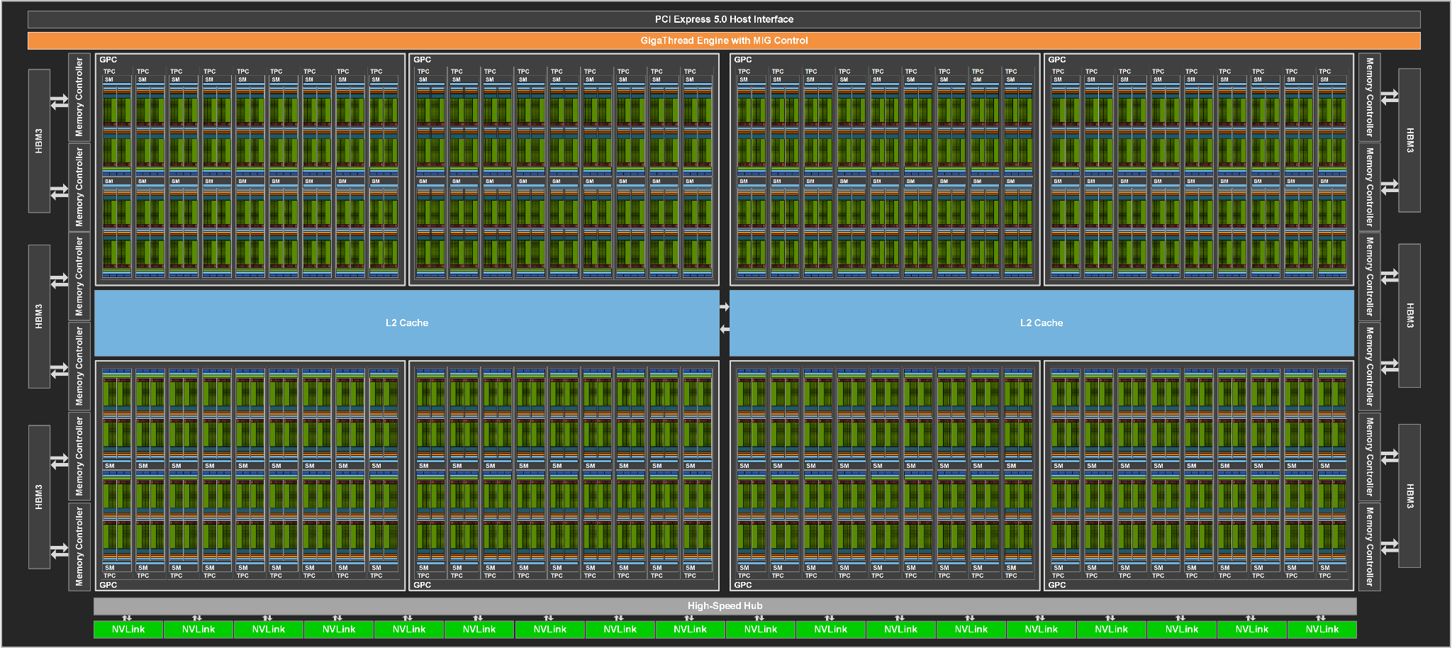
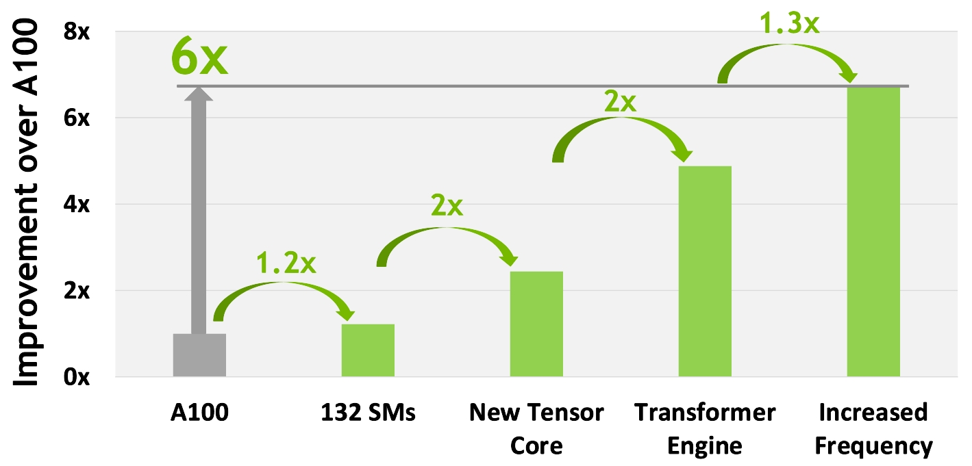
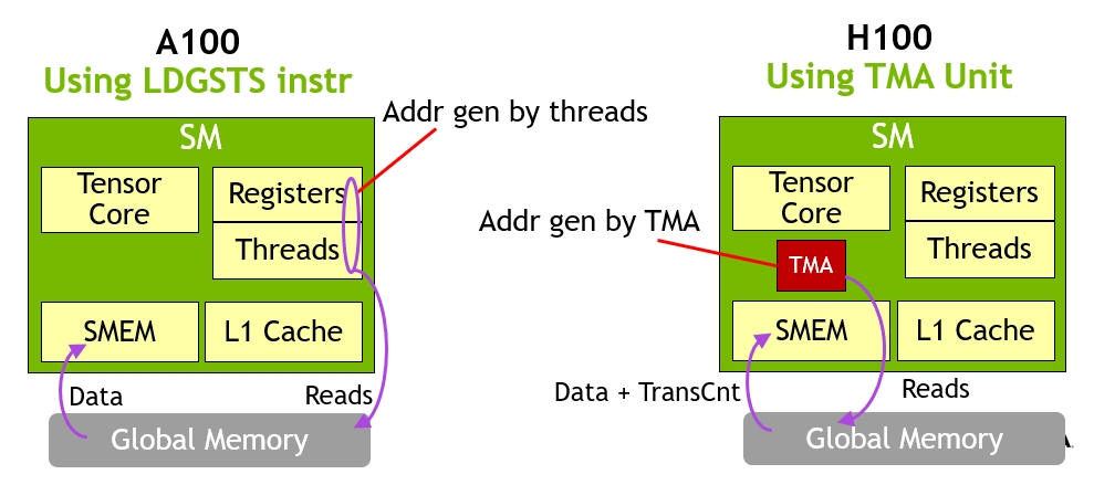
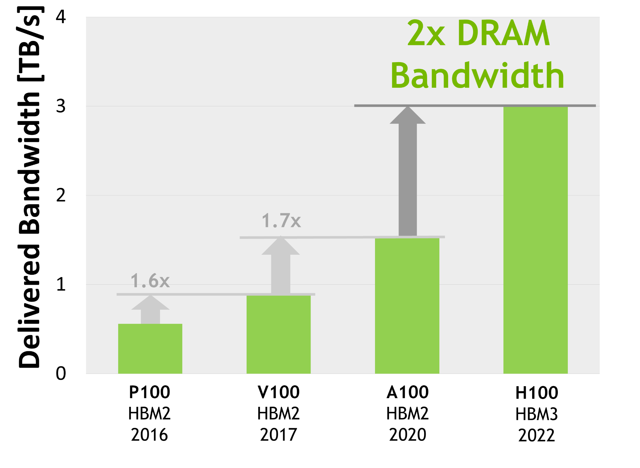
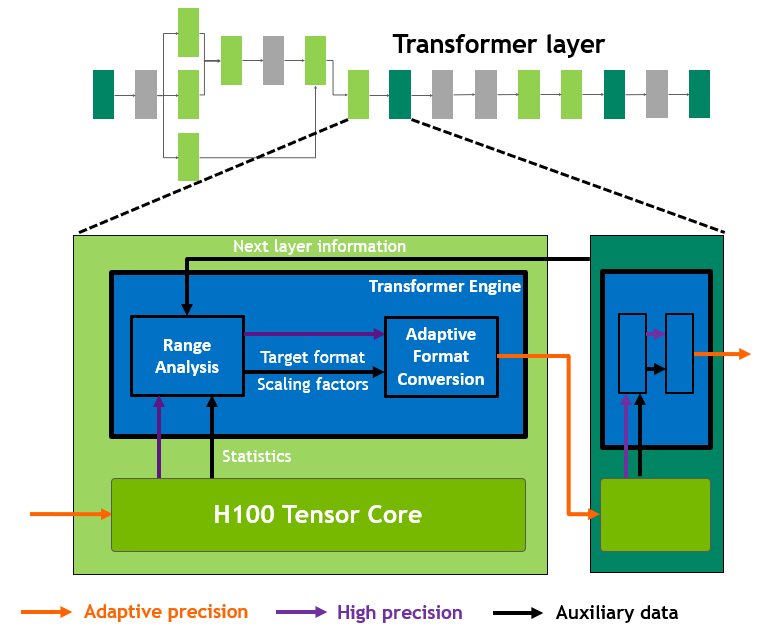
NVIDIA® accelerated computing technologies tackle computational challenges far beyond the capabilities of ordinary computers. New third-generation NVSwitch technology provides hardware acceleration for collective operations with multicast and NVIDIA SHARP in-network reductions; New NVLink Switch System interconnect technology and new second-level NVLink Switches based on third-gen NVSwitch technology introduce address space isolation and protection, enabling up to 32 nodes or 256 GPUs to be connected over NVLink in a 2:1 tapered, fat tree topology These connected nodes are capable of delivering 57.6 TB/sec of all-to-all bandwidth and can supply an incredible one exaFLOP of FP8 sparse AI compute; PCIe Gen 5 provides 128 GB/sec total bandwidth (64 GB/sec in each direction) compared to 64 GB/sec total bandwidth (32GB/sec in each direction) in Gen 4 PCIe. PCIe Gen 5 enables H100 to interface with the highest performing x86 CPUs and SmartNICs / DPUs (Data Processing Units). Hopper’s new fourth-generation Tensor Core, Tensor Memory Accelerator, and many other new SM and general H100 architecture improvements together deliver up to 3x faster HPC and AI performance in many other cases
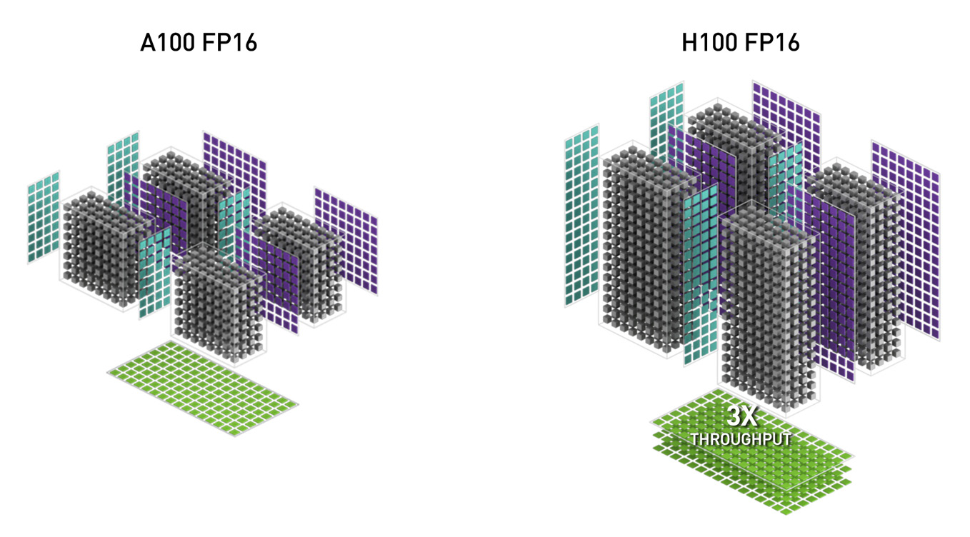
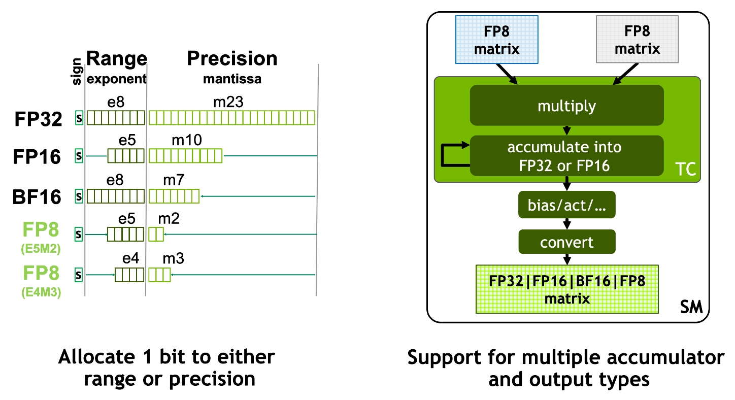
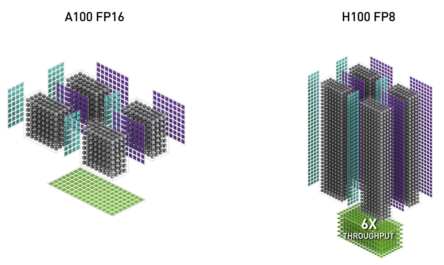
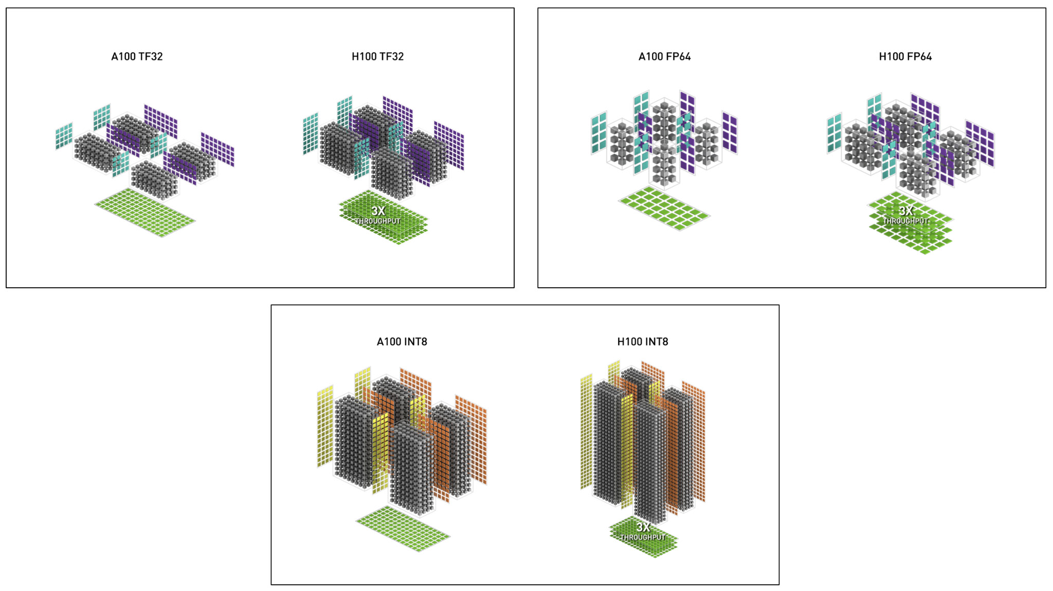
378 TFLOPS | 756 TFLOPS1 756 TFLOPS | 1513 TFLOPS1 756 TFLOPS | 1513 TFLOPS2 1513 TFLOPS | 3026 TFLOPS1. ○ On a per SM basis, the Tensor Cores deliver 2x the MMA (Matrix MultiplyAccumulate) computational rates of the A100 SM on equivalent data types, and 4x the rate of A100 using the new FP8 data type, compared to previous generation 16-bit floating point options. Tensor Cores operating in parallel across SMs in one NVIDIA GPU deliver massive increases in throughput and efficiency compared to standard Floating-Point (FP), Integer (INT), and FMA (Fused Multiply-Accumulate) operations. The new fourth-generation Tensor Core architecture in H100 delivers double the raw dense and sparse matrix math throughput per SM, clock-for-clock, compared to A100, and even more when considering the higher GPU Boost clock of H100 over A100.
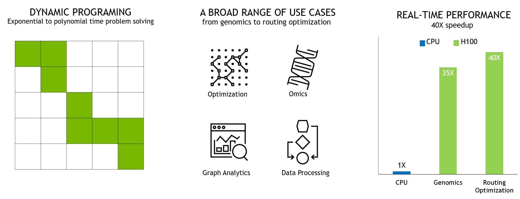
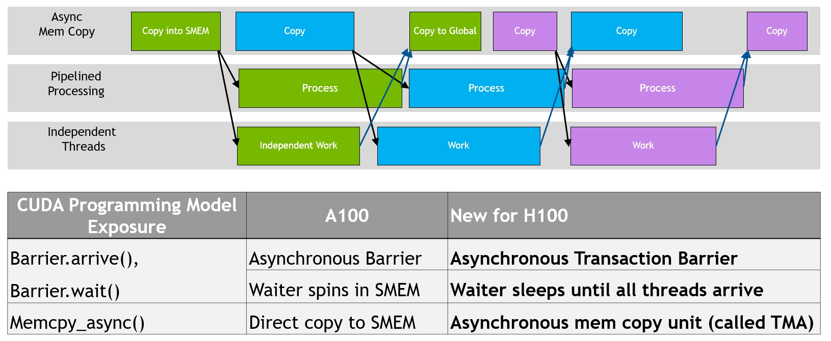
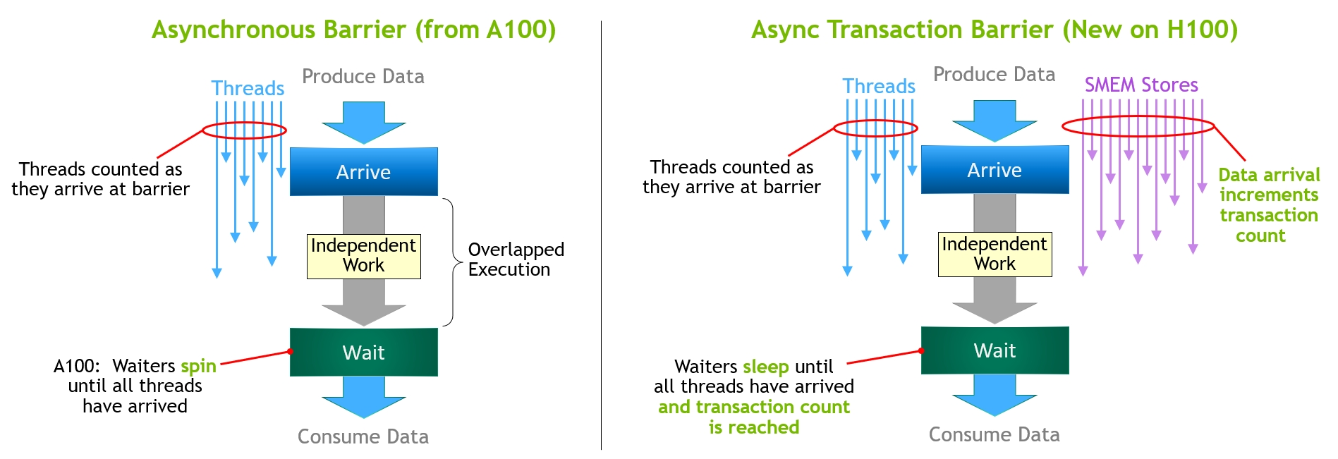
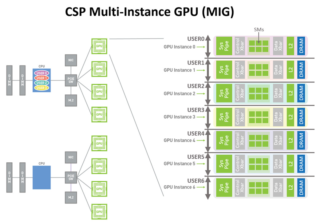
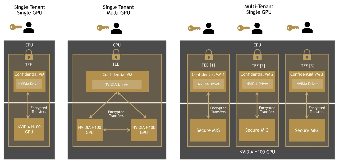
Many “brute force” optimization algorithms have the property that a sub-problem solution is reused many times when solving the larger problem. First introduced in Volta V100, the NVIDIA combined L1 data cache and shared memory subsystem architecture significantly improves performance, while simplifying programming and reducing the tuning required to attain at or near-peak application performance. The Hopper architecture provides new features that improve asynchronous execution and allow further overlap of memory copies with computation and other independent work, while minimizing synchronization points. MIG is especially beneficial for Cloud Service Providers who have multi-tenant use cases, and it ensures one client cannot impact the work or scheduling of other clients, in addition to providing enhanced security and allowing GPU utilization guarantees for customers This CSP MIG diagram shows how multiple independent users from the same or different organizations can be assigned their own dedicated, protected, and isolated GPU Instance within a single physical GPU. The DALI library can be downloaded from https://github.com/NVIDIA/DALI
H100 implements the world's first native Confidential Computing GPU and extends the Trusted Execution Environment with CPUs at full PCIe line rate. ● Fourth-generation NVIDIA NVLink® provides a 3x bandwidth increase on all-reduce operations and a 50% general bandwidth increase over the prior generation NVLink with 900 GB/sec total bandwidth for multi-GPU IO operating at 7x the bandwidth of PCIe Gen 5. ● Third-generation NVSwitch technology includes switches residing both inside and outside of nodes to connect multiple GPUs in servers, clusters, and data center environments. H100 implements the world's first native Confidential Computing GPU and extends the Trusted Execution Environment with CPUs at full PCIe line rate. ● Fourth-generation NVIDIA NVLink® provides a 3x bandwidth increase on all-reduce operations and a 50% general bandwidth increase over the prior generation NVLink with 900 GB/sec total bandwidth for multi-GPU IO operating at 7x the bandwidth of PCIe Gen 5. ● Third-generation NVSwitch technology includes switches residing both inside and outside of nodes to connect multiple GPUs in servers, clusters, and data center environments. The new Tensor Cores have more efficient data management, saving up to 30% operand delivery power
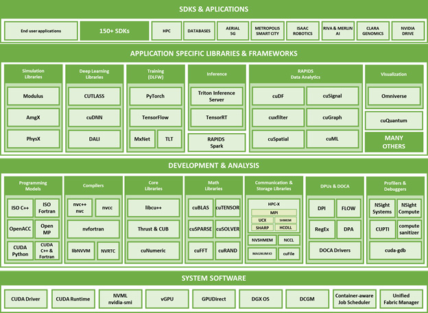
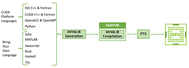
System Memory 1 TB 3200 MHz DDR4 base 2TB config, additional 1TB can be ordered to get to 2TB max Storage. NVIDIA CUDA is a comprehensive, productive, and high-performing platform for accelerated computing It accelerates end-user applications at all levels, from system software to application-specific libraries and frameworks, using GPUs, CPUs, DPUs, and innetwork computing. More than 150 Software Development Kits leverage these libraries to help developers become highly productive in a large set of application domains, including highperformance computing (NVIDIA HPC SDK), AI, Machine Learning, Deep Learning, and Data Science, genomics (NVIDIA CLARA), smart cities (NVIDIA Metropolis), autonomous driving (NVIDIA Drive SDKs), telecoms (NVIDIA Aerial SDK), robotics (NVIDIA Isaac SDK), Cybersecurity (NVIDIA Morpheus SDK), Computer Vision, and many more. LibNVVM is a library for compiling and optimizing NVVM IR to PTX, the virtual ISA of NVIDIA GPUs. All NVIDIA Compute compilers use libNVVM to target NVIDIA GPUs (Figure 32) and it enables users and frameworks to bring their programming language of choice to the CUDA platform with the same code generation quality and optimization as CUDA C++ itself. Other company and product names may be trademarks of the respective companies with which they are associated
- Over 450 NVIDIA SDKs, toolkits, libraries, and models serve industries and applications from gaming and design, to life and earth sciences, robotics, self-driving cars, quantum computing, supply-chain logistics, cybersecurity, 5G, climate science, digital biology, and more. ==Over 25,000 companies use NVIDIA AI technologies today==. The ease of programming and richness of NVIDIA’s CUDA platform allows designers, researchers, and engineers to innovate quickly
- #method/floyd_warshall_algorithm
- #method/transformer_model
- H100 implements the world's first native Confidential Computing GPU and extends the Trusted Execution Environment with CPUs at full PCIe line rate. ● Fourth-generation NVIDIA NVLink® provides a 3x bandwidth increase on all-reduce operations and a 50% general bandwidth increase over the prior generation NVLink with 900 GB/sec total bandwidth for multi-GPU IO operating at 7x the bandwidth of PCIe Gen 5. ● Third-generation NVSwitch technology includes switches residing both inside and outside of nodes to connect multiple GPUs in servers, clusters, and data center environments
- The new Tensor Cores also have more efficient data management, saving up to 30% operand delivery power
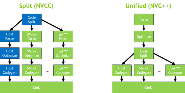
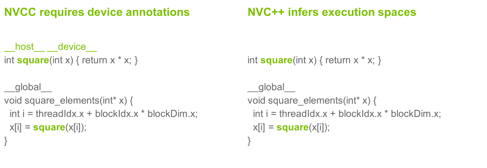
- This model enables certain features that are not available in nvcc